The Ultimate Guide to the 4013HWBC IC: Everything You Need to Know
Introduction to the 4013HWBC
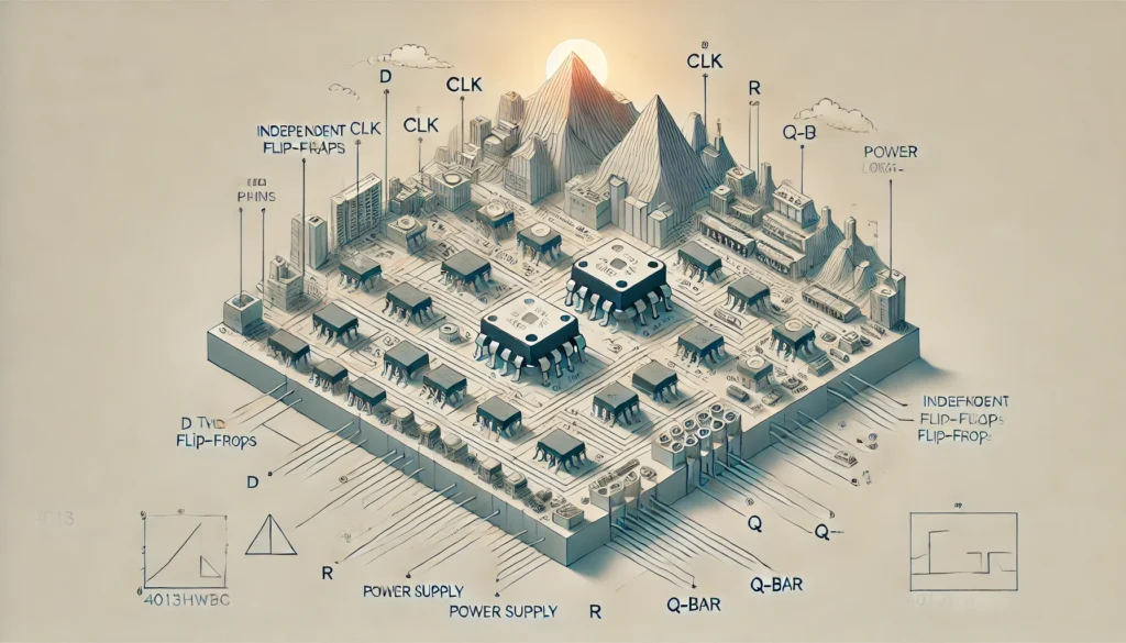
The 4013HWBC is a dual D-type flip-flop IC, widely recognized in the world of digital electronics for its reliability, versatility, and efficiency. Used in both educational projects and commercial applications, this integrated circuit (IC) helps manage digital data by storing bits using flip-flop logic. It is part of the CMOS 4000 series, known for low power consumption and wide operating voltage range.
Whether you are a beginner learning electronics or an engineer developing complex logic systems, understanding the 4013HWBC can significantly enhance your designs.
Technical Specifications of 4013HWBC
This integrated circuit offers a blend of practical features and robust design, making it suitable for various projects. Below is a breakdown of the technical specs:
| Specification | Description |
| Package Type | DIP-14 or SOIC-14 |
| Operating Voltage | 3V to 15V |
| Flip-Flop Count | 2 (Dual D-Type Flip-Flops) |
| Logic Type | CMOS |
| Clock Triggering | Positive Edge |
| Propagation Delay | ~200ns at 10V |
| Power Consumption | Extremely Low |
| Temperature Range | -55°C to +125°C |
These specifications make the 4013HWBC ideal for circuits requiring memory, toggling, or signal division.
Key Features of 4013HWBC
One of the main advantages of the 4013HWBC is its dual flip-flop design. Each flip-flop has data (D), set (S), reset (R), and clock (C) inputs along with complementary outputs (Q and Q-bar).
Dual Independent Flip-Flops
The IC integrates two separate flip-flops, allowing you to handle two data streams simultaneously. Each section can be used independently or linked depending on your circuit requirements.
Wide Voltage and Frequency Range
Supporting a wide voltage range (3V to 15V), it is compatible with various logic levels and battery-powered systems. The IC also handles moderate clock frequencies, ideal for toggling and latching.
Low Power Design
As a CMOS-based IC, the 4013HWBC consumes minimal power, making it ideal for portable or energy-efficient devices.
Applications of the 4013HWBC
The 4013HWBC is a fundamental building block in numerous digital systems. Here are some of the most common applications:
- Frequency Dividers: Each flip-flop can divide the clock frequency by 2, making it useful in timers and counters.
- Data Storage: Temporarily stores 1-bit data for use in sequential circuits.
- Toggle Switches: Used in push-button toggles for digital on/off switching.
- Debouncing Circuits: Helps clean up noisy signals from mechanical switches.
- Shift Registers: Part of complex data transfer operations between devices.
These applications show just how versatile and indispensable the 4013HWBC can be in digital electronics.
Benefits of Using the 4013HWBC
Choosing the 4013HWBC IC in your projects offers multiple advantages that go beyond its basic flip-flop function:
- Ease of Use: Clearly labeled pins and standard logic behavior make it beginner-friendly.
- Cost Effective: Its affordability makes it suitable for mass production and educational kits.
- Compatibility: Works with other CMOS and TTL logic components.
- Stable and Reliable: Once latched, the data output remains consistent until the next clock cycle or reset.
Its adaptability makes it a staple in labs, classrooms, and commercial devices.
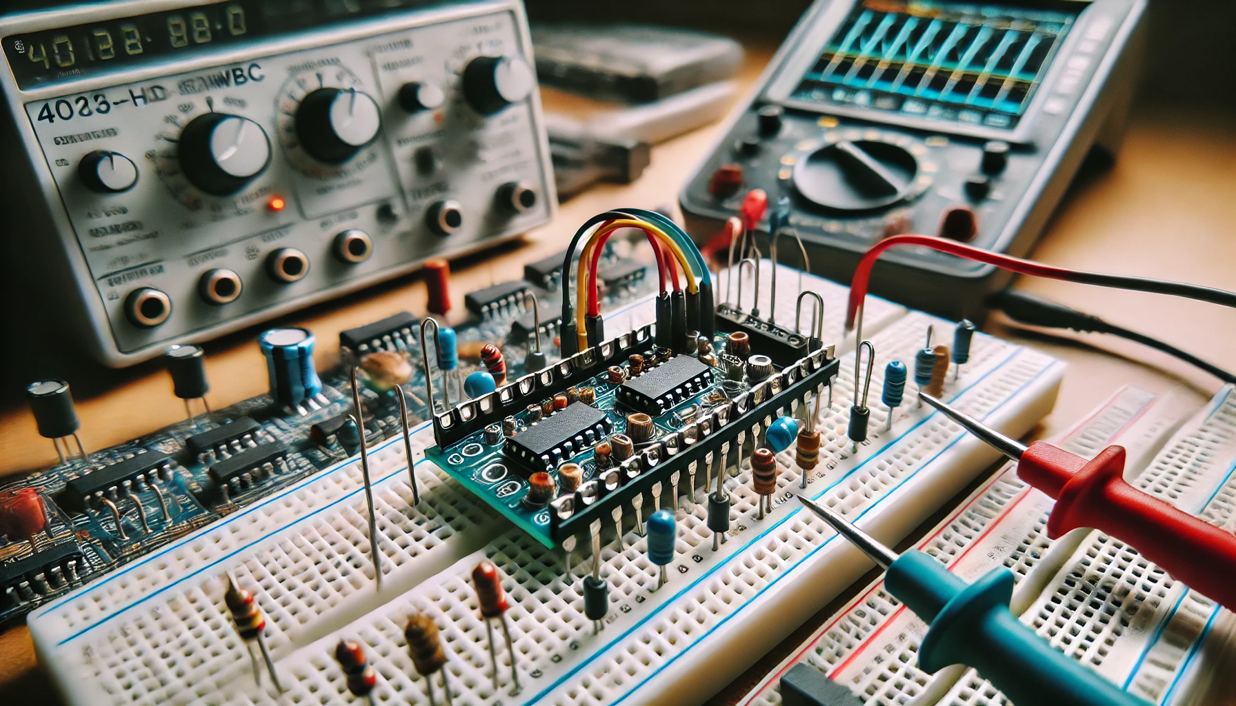
Best Practices for Using the 4013HWBC
To get the best performance from the 4013HWBC, consider these tips:
- Use Decoupling Capacitors: Place a 0.1µF ceramic capacitor close to the Vcc pin to filter out voltage spikes.
- Debounce Inputs: When using mechanical switches for clock or reset, include debouncing logic or filters.
- Observe Pin Configuration: Incorrect wiring can lead to erratic behavior or permanent damage.
- Avoid Floating Inputs: Tie unused inputs to ground or Vcc through a resistor to prevent instability.
Following these guidelines will help you create stable and efficient designs.
Why Choose the 4013HWBC Over Alternatives?
Compared to other flip-flop ICs, the 4013HWBC offers a solid balance between performance, cost, and versatility. While other ICs may specialize in high-speed operations or different triggering methods, this IC remains a go-to option for most general-purpose digital needs.
Its low power usage, dual functionality, and easy integration make it a practical choice across a broad range of industries and educational settings.
FAQs
1. What is the maximum clock frequency the 4013HWBC can handle?
While it varies by voltage, the IC typically handles clock speeds up to a few MHz. Always refer to the datasheet for exact specs.
2. Can I cascade multiple 4013HWBC ICs?
Yes, you can chain them for more complex logic operations, such as 4-bit or 8-bit storage and counters.
3. Does the IC require external pull-up resistors?
Not usually, but for certain setups like open-collector outputs, pull-ups may be beneficial.
4. How should I store the IC to prevent damage?
Store in anti-static bags in a dry, room-temperature environment to avoid electrostatic discharge and moisture damage.
5. What is the lifespan of a 4013HWBC IC?
Under normal operating conditions, it can last for decades without degradation, thanks to its robust CMOS construction.
Conclusion
The 4013HWBC IC is a powerful yet easy-to-use component that plays a vital role in digital circuit design. With its dual flip-flop configuration, low power consumption, and flexible application range, it’s no surprise this IC remains a favorite among students and engineers alike. Whether you’re developing a toggle switch or creating a data storage system, the 4013HWBC delivers performance and reliability in one small package. If you’re aiming for a cost-effective, low-power, and user-friendly logic component, this IC should be at the top of your list.
Recommended Articles
The Ultimate Guide to the Songbird Serenade AI Voice Model
NBA 2K23 Chuma Okeke Cyberface: The Ultimate Guide to His Realistic In-Game Look